Search This Blog

Saturday, April 19, 2014

Nuclear Research Reactors - MK 1 - Testing Radiation Hardening

Satellites that are flown into orbit face radiation that can damage their electronic components and render the satellite useless.  Modern semiconductors are very susceptible to damage from ionizing radiation, both electromagnetic and charged particles.  Electronics that are flown into space (whether deep-space probes, communtications satellites, etc.) face much harsher radiation fields than they would under the protective atmosphere of mother earth.

Radiation can damage electronics in several ways.  Here are a list of naturally-occuring types of radiation that can affect an object in space: (From Wikipedia)

  • Cosmic rays come from all directions and consist of approximately 85% protons, 14% alpha particles, and 1% heavy ions, together with x-ray and gamma-ray radiation. Most effects are caused by particles with energies between 108 and 2*1010 eV. The atmosphere filters most of these, so they are primarily a concern for spacecraft and high-altitude aircraft.
  • Solar particle events come from the direction of the sun and consist of a large flux of high-energy (several GeV) protons and heavy ions, again accompanied by x-ray radiation.
  • Van Allen radiation belts contain electrons (up to about 10 MeV) and protons (up to 100s MeV) trapped in the geomagnetic field. The particle flux in the regions farther from the Earth can vary wildly depending on the actual conditions of the sun and the magnetosphere. Due to their position they pose a concern for satellites.
  • Secondary particles result from interaction of other kinds of radiation with structures around the electronic devices.

  • There are several other types of radiation that can damage electronics that are man-made, or that occur on earth.  But for simplicity in this post, I am restricting the discussion to those radiation sources that naturally occur in space.

    There are a number of cool techniques electronics manufacturers use to reduce damage caused by radiation, and to make the chips more tolerant to the damage that will eventually occur: (Again from Wikipedia):

  • Physical:
    • Hardened chips are often manufactured on insulating substrates instead of the usual semiconductor wafers. Silicon on Insulator (SOI) and sapphire (SOS) are commonly used. While normal commercial-grade chips can withstand between 50 and 100 gray (5 and 10 krad), space-grade SOI and SOS chips can survive doses many orders of magnitude greater. At one time many 4000 series chips were available in radiation-hardened versions (RadHard).[3]
    • Bipolar integrated circuits generally have higher radiation tolerance than CMOS circuits. The low-power Schottky (LS) 5400 series can withstand 1000 krad, and many ECL devices can withstand 10 000 krad.[3]
    • Magnetoresistive RAM, or MRAM, is considered a likely candidate to provide radiation hardened, rewritable, non-volatile conductor memory. Physical principles and early tests suggest that MRAM is not susceptible to ionization-induced data loss.
    • Shielding the package against radioactivity, to reduce exposure of the bare device.
    • Capacitor-based DRAM is often replaced by more rugged (but larger, and more expensive) SRAM.
    • Choice of substrate with wide band gap, which gives it higher tolerance to deep-level defects; e.g. silicon carbide or gallium nitride.
    • Shielding the chips themselves by use of depleted boron (consisting only of isotope Boron-11) in the borophosphosilicate glass passivation layer protecting the chips, as boron-10 readily captures neutrons and undergoes alpha decay (see soft error).
  • Logical:
    • Error correcting memory uses additional parity bits to check for and possibly correct corrupted data. Since radiation effects damage the memory content even when the system is not accessing the RAM, a "scrubber" circuit must continuously sweep the RAM; reading out the data, checking the parity for data errors, then writing back any corrections to the RAM.
    • Redundant elements can be used at the system level. Three separate microprocessor boards may independently compute an answer to a calculation and compare their answers. Any system that produces a minority result will recalculate. Logic may be added such that if repeated errors occur from the same system, that board is shut down.
    • Redundant elements may be used at the circuit level. A single bit may be replaced with three bits and separate "voting logic" for each bit to continuously determine its result. This increases area of a chip design by a factor of 5, so must be reserved for smaller designs. But it has the secondary advantage of also being "fail-safe" in real time. In the event of a single-bit failure (which may be unrelated to radiation), the voting logic will continue to produce the correct result without resorting to a watchdog timer. System level voting between three separate processor systems will generally need to use some circuit-level voting logic to perform the votes between the three processor systems.
    • Hardened latches may be used.
    • A watchdog timer will perform a hard reset of a system unless some sequence is performed that generally indicates the system is alive, such as a write operation from an onboard processor. During normal operation, software schedules a write to the watchdog timer at regular intervals to prevent the timer from running out. If radiation causes the processor to operate incorrectly, it is unlikely the software will work correctly enough to clear the watchdog timer. The watchdog eventually times out and forces a hard reset to the system. This is considered a last resort to other methods of radiation hardening.

  • The bottom line is that you want to ensure all the efforts you have made above to ensure your circuits are safe against radiation is to test them *before* you put them into an expensive satellite and send it up into space.

    One of our customers was a large aerospace company that flew communications satellites, and needed to test their hardware for radiation hardness.  We provided them with a cadmium-lined dry tube that went directly into the MK 1 reactor core. 

    The cadmium inside the tube absorbed thermal neutrons (which don't exist in outer space), and allowed the gamma and fast neutrons to zap the circuits.  The calculation by our reactor physicist was that 30 minutes at 10 watts would be a lifetime worth of radiation damage in outer space. 

    The engineer lowered his assemblies, connected by wires to an oscilloscope, to the bottom of the tube, and I ran the reactor for him.  I never was able to get an answer from the engineer how well his circuits held up.  Perhaps he was working on a government project, and was sworn to secrecy...

    ... or maybe he just wasn't chatty.  Who knows? :)

    Saturday, April 05, 2014

    Nuclear Research Reactors - TRIGA MK 1 - Neutron Radiography

    The TRIGA MK 1 was most often used to do Neutron Activation Analysis when I was at the facility.  However there were some other uses to which it could be put.  From time to time the MK 1 was used for neutron radiography.

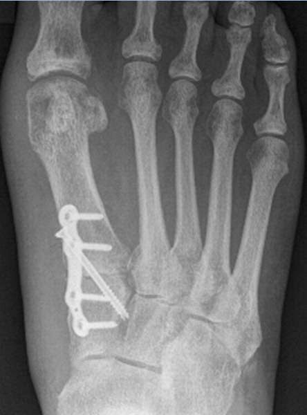
    Most people are familiar with X-ray photography, and have seen pictures of broken bones, devices used to knit bones together, and pacemakers.  Everyone has seen X-ray pictures.  See below for a few examples (Click any image to enlarge).

    Broken Leg

     Broken Big toe, with plate and a drywall screw

     Pacemaker with stimulating wires

    X-rays are ideal for taking pictures of things that absorb X-rays, such as bone and metal.  But if you need to look inside something made of metal... what then?  X-rays won't make it through to the other side because they will be absorbed.  Suppose we were to use neutrons instead?

    Neutrons will go right through some metals and let you look at what is inside, because neutrons are absorbed by a different mechanism than X-rays.  For example, if you wanted to image a rubber band inside of a lead brick, X-rays would be useless, but neutrons could do that.  Let's look at a couple of examples of neutron radiography.

    Below:  An X-Ray image of a 35mm SLR camera:  Note the lack of detail and large dark areas where metal has blocked the X-rays from reaching the film.

    Below:  The same camera, this time imaged using Neutron Radiography.  Many more of the details of the internals are visible.  The darker items in this image will tend to be plastics and other materials that contain hydrogen atoms.

    Below is a somewhat blurry image of an air compressor.  Even with the blur, you can make out the crankshaft, connecting rod, wrist pin, valves, and even the roller bearings.  Try doing that with X-rays.


     My favorite.  A motorcycle engine.  You can see the intake valve to the right, exhaust valve to the left, valve seats, valve springs, the sparkplug, the piston rings, the piston and wrist pin, the connecting rod, and the bolts holding the thing together.  You can even specks of corrosion or carbon buildup on the piston skirt.  The resolution far surpasses most X-ray images.

    The only problem with neutron radiography is that you can't use it on living tissue.  Neutrons are pretty lethal, and they also get absorbed, making things radioactive.  Additionally, people, being mostly water, are opaque to neutrons.  Nevertheless, neutron radiography is a very useful tool for imaging the inside of metallic objects.

    The way neutron radiography was accomplished at the facility is thus:  A 12"x12" square aluminum dry tube was placed in the reactor pool, next to the core.  The dry tube was 25 feet long so that it could reach the bottom of the pool and sit close to the reactor core. 

    The dry tube gave neutrons (and unwanted gamma radiation) a path to escape the core without being absorbed in water.  The length of the tube served to "collimate" the neutrons - to have them traveling in the same direction as they exited the top.  This collimation helps to sharpen the image.  

    At the top of the tube would be a thin aluminum plate, upon which the item to be imaged rested.  Just above the item would be an aluminum cassette containing a large piece of photographic film.  I no longer recall if it was special film or just ordinary X-ray film.  The reactor power level required for this process wasn't terribly high - perhaps 5 watts for 10 minutes exposure time.  However just 5 watts of unshielded radiation straight up from the reactor core is a nasty dose.

    While performing neutron radiography, the receptionist was required to leave the building, since she was not a trained Radiation Worker.  I wasn't keen on getting dosed with neutron and gamma either, and I was a lot closer to the dry tube than the receptionist desk.  Fortunately, this was an infrequent operation, so it probably wasn't necessary to move the reactor control console to a separate room.

    Neutron radiography is a very cool imaging technique, with some useful real-world applications. 

    The Air Force's F-111 Aardvark (as well as other aircraft) had aluminum honeycomb structure inside the wings for stiffness.  It was found that corrosion was occurring within the honeycomb.  It would have been incredibly tedious and expensive to peel back the skin of every F-111 wing at maintenance intervals to perform a visual inspection.  Instead, the Air Force used neutron radiography with a new TRIGA reactor at McClellan Air Force Base in Sacramento. 

    The more you know!  

    Nuclear Research Reactors - MK 1 - Neutron Activation Analysis

    General Atomics owned and operated the very first TRIGA reactor between 1958 and 1997.  It was  called the MK 1, and was the brain-child of the awesome physicist Freeman Dyson (NOT the  vacuum-cleaner sales guy).  The reactor has since been decommissioned and I believe is now a technological historic site.

    Thursday, April 03, 2014

    Nuclear Research Reactors - The MK 4 Experiments *UPDATED*

    I was a reactor operator at General Atomics in the late 1980's.  General Atomics then operated two swimming-pool type TRIGA reactors.  The first was a MK IV reactor that was the bread and butter of the reactor division of the company.  It had two long-running experiments, one of which piggy-backed on the primary one.

    Below, a TRIGA reactor similar to the one I operated.  Yes, it glows just like that!


    The primary experiment that the MK IV was used for was in-core thermionic cell testing.  The goal of testing the thermionic cells was to determine the longevity of these unique devices. 

    What the heck is a thermionic cell?  In order to explain, we need to understand how a basic vacuum tube works.

    Below is a diagram of a vacuum tube called a diode.  It has two elements inside the glass tube (the circle).  These elements are called the cathode and the anode.  I prefer to call them an emitter and a collector.  In this diagram, the bottom emitter is heated by an electrical current, labeled "Filament Supply".  So - there is a short electrical loop completely dedicated to heating the spiral-wound filament, which is made of tungsten.  Tungsten is chosen because it ejects electrons when heated.  This process is called "Thermionic Emission"

    Next, voltage is applied at the right side of the diagram, to put a positive charge on the Anode (collector), and a negative charge on the cathode (emitter).  This causes electrical current to flow from the emitter at the bottom, to the collector at the top, just like it were a piece of copper wire.

    Current will not flow in the other direction if the voltage on the right is reversed though, because the anode is not a heated piece of tungsten, ready to fling electrons out.  This is the simplest vacuum tube around.  It is called a diode, and it only lets current pass in one direction, from cathode (emitter) to anode (collector).


    So with this understanding of a basic vacuum tube, let's see if we can figure out a thermionic cell.

    Suppose in our drawing above, we crank up the power provided by "Filament Supply", so the tungsten emitter is really blasting electrons out.  Next, we put the emitter in the center of the vacuum tube, and the collector encircles it, so that no matter what direction the electrons go, the anode (collector) will capture them.  This process is called thermionic conversion.  You heat the cathode hot enough and it kicks out electrons, and now you have DC current from cathode (emitter) to anode (collector).  On the right side of our drawing above, you could power a light bulb with this current.

    The clever part of thermionic conversion is you get DC power without the need for a boiler, steam turbine, generator, condenser, pumps, etc, etc.  It's a pretty simple and elegant arrangement.

    In a nuclear thermionic cell, the emitter is a small thimble of uranium that is coated with tungsten.  Around the emitter is a slightly larger collector.  The assembly is placed in a reactor.  Fission begins in the uranium, which in turn heats the tungsten coating.  The tungsten ejects electrons, and current flows in the thermionic cell.  Even a tiny thermionic cell can generate 1KW of low-voltage but high amperage power.

    Below:  A top-down cutaway of a nuclear thermionic cell.  The cathode is made from tungsten-coated enriched uranium and inserted into a reactor.


    If you had enough of these devices in a single small reactor core, you could easily get a Megawatt of power.  This would be perfect to launch into orbit as a power supply for your space laserplasma weapon, or coil gun to shoot down incoming nuclear missiles - and in fact the project was funded by the Department of Defense through the Strategic Defense Initiative (aka the "Star Wars" Program).

    The MK IV reactor was run round the clock in order to put reactor hours on the thermionic devices, to see how they would hold up, year after year. 

    We had some other people who wanted to use the MK IV reactor's spare neutrons, and run their "experiment" alongside the thermionic experiment.  These guys were jewelers.  That's right, they made jewelry.  I don't think the jewelers had the income stream to keep the reactor running 24-7, so it was good that they could use the opportunity provided by the government's experiment.

    This is where I learned about gemstone color enhancement.  Improving the appearance of gemstones goes back to ancient times, when emeralds would be soaked in oil to hide their fractures.  Nowadays though, a generic stone like topaz can be made beautiful by irradiation. 

    The stones were packed into canisters and placed in dry Cadmium-lined tubes (to provide fast neutron flux only).  Even with fast neutron flux, due to trace impurities in the stones, they become radioactive during the process.  The jewelers would come in once a week and rotate the stones using remote tools, so that the stones would be irradiated from all sides.  After the stones were cooked, they would be removed from the reactor, but left on a shelf well below the water level, because they were quite radioactive, fresh out of the core.

     It would take quite a while for the radioactivity to die off enough for the stones to be released to the public.  The jewelers probably had 5-10 million dollar's worth of inventory stacked out in cheap sheet-metal lockers at a given time, waiting for the activity to fade. 

     Here is a raw uncut, uncolored topaz, as you would find it in nature.  Not impressive.


    Below is a cut natural topaz.  Nice clarity and cut, but I am not a fan of pee-yellow gemstones, and most others aren't either.

     Below is a Topaz that has been irradiated with fast neutrons.  This color is called "London Blue", or "Swiss Blue", and is actually about the color of Windex glass cleaner.

    Below is a Topaz that has been irradiated by fast neutrons, and afterwards been irradiated by an electron beam provided by a linear accelerator.  I like this color better, and the jewelers started producing these after a while.  I helped install a used linear accelerator in the underground bunker.


     Below is the "Sky Blue" color you get when you irradiate a topaz with pure gamma rays from a Cobalt-60 source.  Pretty.  Also no neutrons, no radioactivity.  You can wear it the next day.

    As always, fascinating stuff!

    ****UPDATE****

    An interested anonymous commenter has graciously done a lot of homework and helped out with content on the Gemstone Color Enhancement process.  Thank you for that!

    Here is a great link for a layman explaining how the various color shifts are achieved

    Here is a cool research paper with experiments showing gemstone color changes with dose

    Some early (1981) irradiated topaz stones were released before the radioactivity had died down

    A nice long-form explanation of topaz color enhancement

    Lastly, the link where all the above links (and many more) Can be found:

    All very cool information!  Thanks again Anon commenter :)

    Wednesday, April 02, 2014

    A few recent photos

    Today I got around to pulling a few photos off a little camera we use around the house.  It's been a while since I cleared the memory card out.

    I did find a few cool pictures on it though, and thought it would be good to share them.

    Below is a picture taken from Schweitzer Mountain Ski Resort.  At the foot of the mountain is the town of Sandpoint, ID and the northernmost end of Lake Pend O'reille (pronounced Ponderay).  The sky looks threatening, and it was.  About 5 minutes after I took this picture, really heavy snow started falling.


     This is a look out our front door following the last big snowstorm we had this year.  We cut a little path off the left side of the walkway so we can reach the satellite dish to clear snow off it.  Franky I was ready for winter to be over with BEFORE this last foot of snow hit.

    
     The back yard.  No shoveling required!!!

     
    A Northern Flicker (a woodpecker), in for lunch.  He wasn't keen on having his picture taken and kept ducking behind the tree.